_TOP_MENU

Feb 24, 2014

Coverage Analysis


Coverage Analysis  

First question,

why coverage analysis is important for a design ?

What are the inputs in coverage analysis and what outputs will get after doing coverage analysis ?


Answers are , Coverage analysis is a important part in Design and Verification , this give us the visibility inside design that how much code is verified and how much is left.

Coverage are two types.
1. Functional Coverage
2. Code Coverage

Functional Coverage 

Functional coverage is coverage which tell you how much functionality is covered in  ( design or verification ?? )  .....  it is design , verification is done to cover all functionality of design. For analysis, if verification environment is random constraint based testing then functional coverage should be measured by using cover points.
If verification environment is direct testcase based testing , then one can make XLS and put the testcase name , but this will be more documentation purpose and will not tell you actual functional coverage.


Code Coverage 

Code Coverage will tell you that how much RTL is verified and how much is left .. This will also tell you some corner cases which didn;t cover in verification.

Code Coverage is summation of different type of coverage , few important are -
statement coverage
expression coverage
FSM coverage
branch coverage
toggle coverage
etc ..

All are important and should be close to 100% but statement and FSM coverage should be 100%.


Feb 13, 2014

BIST - Built-in-self-Test


BIST generates its own stimulus and analyzes its own response.  BIST is used normally to validate a product in labs, there are different kind of BIST used in system to validate.
one of the method is , using LFSR, LFSR generates random stimulus and it is expected that chip is in its normal functional mode. with the configuration, with LFSR , one can validate the data path in system or in IP.


What is the motivation for BIST ? 
-> cost-efficient testing
-> stuck-at-fault model
-> cost of ATE (Automatic Test Equipment)


Types of BIST  

-> on-line BIST 
->  Concurrent on-line BIST 
Occurs simultaneously with normal functional operation , normally coding techniques or duplication and comparison are used.

           
 ->   Non-concurrent on-line BIST 
Carried out while in idle state , by executing software or firmware routines .

-> off-line BIST
System is not in its normal functional mode.

-> Functional off-line BIST 
It is based on a functional description of the circuit under test and uses functional high level fault models.
 

-> Structural off-line BIST 
Execution based on the structure of the circuit under test and used structural fault models.
Example -  Stuck-At-Fault  (SAF)  - cell stuck at constant value
                  Transition Fault  (TF)    - a cell which fails to go from 0->1 or 1->0  transition
                  Coupling Fault (CF)     - write operation to one cell changes the contents of a second cell

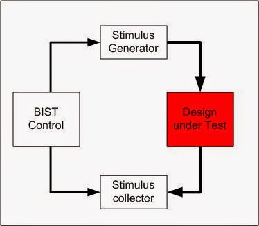
General Architecture of BIST 

Below is typical architecture of BIST testing , bist generator and bist collector would be inside DUT or outside DUT , depends on the BIST type.


LFSR Based Testing  : 

LFSR :  Linear Feedback Shift Register , hardware that generates psedo-random pattern for CUT (circuit under test)

BILBO : Built-In logic block observer , extra hardware need to convert flip-flop into scan chain in test mode.
Exhaustive Testing  : Apply all possible 2 (power of) n pattern to a circuit with n inputs , this will take more ATE time.

Pseudo-exhaustive testing:  Break circuit into small , overlapping blocks and test it.

Psudo Random test generation :


PRBS is basically a polynomial having a standard definition,  for exam - PRBS7, PRBS8, PRBS10, PRBS 31 ..

higher the number of PRBS, pattern will be more random and possibilities to hit a expected pattern in pattern generation will increased.

below is one example of implementation of polynomial, if you are more interested to go in more deep, send a email to me.


Ref -
http://en.wikipedia.org/wiki/Built-in_self-test
http://www.asic.co.in/ppt/BIST2.pdf

Feb 6, 2014

Static Timing Analysis


STA play an important role during chip development process, it is timing sign off process.


So .. What is STA ?
Static timing analysis (STA) is a simulation method of computing the expected timing of a digital circuit without requiring a simulation of the full circuit. High-performance integrated circuits have traditionally been characterized by the clock frequency at which they operate.

Below are the main responsibilities of a STA engineer.

1. Setup Timing violations
2. Hold Timing violations
3. Min Pulse violations
4. Max transition violations
5. Max Cap violations
6. Clock transition violations
7. Clock Gating violations .. etc

Hold timing check can only be done once clock tree netlist is available. Hold time is not dependent on clock frequency.
Setup timing can be check on after synthesis netlist with more margin. It will give initial report about the design.

There could be n number of corners , below is the calculation for corners.

STA run individually in test mode and function mode.

Test Mode ->
These days there could be below test mode.
1. Scan mode
2. At-Speed/Capture mode.
3. OCC scan mode

Functional Mode ->
It depends on the functionality of design. There could be normal mode, loopback mode , few special debugging mode .. , when design is not in test mode, design support one mode at the time.
1. normal mode
2. Loopback mode

PVT conditions ->
1. Fast corner ( best case)
2. Slow corner (worst caese)
3. Fast corner with higher temp
4. Typical
5. combinations of corner 1 and 2

Total corners -> (number of PVT condition) * (Functional Mode) * (Test mode)

Once STA has ran , post processing will required to get the desired result. If using some standard tools which can present a dashboard from STA result , then much scripting may not be required.

Perl/Tcl is majority of script which used in post-processing and building up the environment. Shell can also be used.

You need to have good grip on below unix command.
1. grep
2. compare
3. find
4. awk
5. sed

Under-Construction Pages :
Timing Analysis : Input to output
Timing Analysis : Input to Reg
Timing Analysis : Reg to Reg
Timing Analysis : Reg to Output timing analysis


For go in more detail, go @ below link.

Practical Knowledge on STA

FAQ :
Q1. how to get the unconstrained path in a design ?
A. check_timing -verbose
     report_timing -exceptions
     report_disable_timing

Q2. What is the relationship for the timing analysis and UPF ?
A.  ??


Thanks
Rahul


Feb 5, 2014

Timing Constraint


Below are the basic commands in constraint file.

1. current_instance  -- Sets the current instance of design.
Example  -   /design/ins1/moduleA

2. set_hierarchy_separator  -- Specifies the hierarchy separator used in SDC file.
Example -
set_hierarchy_separator .
set_hierarchy_separator /

all_clocks
all_inputs
all_outputs
all_registers -clock CLK1

current_design 


create_clock  
This will define the clock , simple syntax to define clock is
create_clock -period [get_ports <CLK>]
user can define custom clock also, like define the duty cycle if it is not 50/50. also one can define the multiple rising edge , falling edge within one clock period using -waveform {.. ,..}


create_generated_clock
A generated clock is a clock derived from a master clock. master clock is define using create_clock.
In Design , in clocking architecture, multiple clock can be derived from one master clock, and generated could be a divided version of master clock or could be a multiplier version of master clock. either one can be defined using -multiply_by or -divide_by option. 


set_clock_latency

There are two types of clock latency ,
1. source latency  - also called insertion delay , this is the delay from clock source to clock definition point.
2. network latency - network latency is the delay from clock definition point to the clock input of flop.
The total clock latency is the sum of both , network latency and source latency.example is given below.

# Rise clock latency on CLK_A is 1ns:
set_clock_latency 1.0 -rise [get_clocks CLK_A]
# Fall clock latency on all clocks is 1.2ns:
set_clock_latency 1.2 -fall [all_clocks]

clock latency


set_clock_sense

set_clock_uncertainty
clock uncertainty is the time in clock period which used to model clock jitter and other pessimism factor during the timing analysis.
Example  -
set_clock_uncertainty -setup 0.1 [get_clocks CLK_A]
set_clock_uncertainty -hold 0.05 [get_clocks CLK_A]

set_data_check

set_disable_timing

set_false_path

set_ideal_latency

set_ideal_network

set_ideal_transition

set_input_delay

set_max_delay

set_max_time_borrow

set_min_delay

set_multicycle_path  (important one)

set_output_delay

set_case_analysis

set_driving_cell

set_fanout_load

set_load

set_max_fanout

set_max_transition

set_operating_condition (optional)


set_clock_groups 
You can use either one of option depends on the functionality and clock muxing in design.
physically_exclusive means that particular clocks will never be present physically at the same time , logically_exclusive means particular clocks will be available but will never used at the same time. this helps in crosstalk analysis between the clocks , as if clocks are physically available on board then there will be noise and crosstalk associated with it.

set_false_path is having the same thing as logically_exclusive , either one of them can be used to remove false paths from timing analysis and reports.

1.) Looks like you are mixing set_false_path and set_clock_groups. Both of them are very different and typically you don't need both at the same time in a certain section of the design.
The whole idea behind set_clock_groups is to make timing paths go away (i.e. not show up in reports - so in that sense it is similar to false paths, but both these commands have very different purposes).
All 3 options i.e. -asyn -phys_excl and -logic_exl will cause no paths to show up. So there is no need for an explicit false path if you are able to use set_clock_groups.

2.) The differenece between -async and -log_excl is in the way, PT handles crosstalk analysis.
If 2 clocks are async, it means that they don't have any phase relationship at all. So instead of using definite timing windows based on arrival times/skew etc, the tool will use infinite timing windows when calculating aggressors and victims,

When you use -logic_excl switch, it still means that no timing paths will show up, however crosstalk analysis will be done with regular timing windows based on arrival times/skew etc.

Practical Example of Timing Constraint like on I2C/SPI/etc 

----------------------
Feb 4, 2014

How to debug functional simulation

Few points before heading towards simulation debug -

1. Ask yourself, do you know what is the DUT ?
2. Do you have enough information , what is the driving signals and what signals to monitor?
3. Do you have enough information about the verification environment ?


If your answer is yes for all of 3 questions , then you can go through the steps mentioned below , and if your answer is "NO" for any of the question .. I know you will go through the steps below to know how to debug a simulation. :)  not an issue , it's human nature.

 I think it's good if you know the verification environment. What testbench is driving to DUT and what
 response is expected from DUT.

Go through the below steps :-

1.  Try to identify issue , it could be in testbench or DUT , make sure either one is correct and behaving as expected.
2. If issue is in DUT, then try to break your testcase , identify which part of testcase is failing.
3. Once you know functionality A is not working in Dut, then may be fix RTL if you have RTL and confirmed that issue is in RTL.
4. if you are working on IP level , then it is easy to debug. But at SoC level, it becomes very difficult to identify issue and debugging due to simulation time and simulation dump size.
5. If simulation time is very big, then optimized initial startup sequence , some of functionality may not required and can be skipped during debugging.
6. Dump signals which are required , do not dump all signals in design.
7. For modelsim/Questa, you can make .do file , which can have particular signals required in debugging.
8. Always dump common buses where you can see the traffic going in/out inside DUT, this will help to understand the failure case and time.

I think knowing the environment is the key point. Even if you dont know much about the DUT , you can still confirm with designer that there is bug in DUT.
To know more about the Verification environment , go through the below link.
Verification Environment

As usual , comments are most welcome and if any one want to add something, please put on comment. I will try my best to keep this thread alive.

Thanks a lot.

Feb 3, 2014

Contents


Below are the main topics to be discussed and professional will have advantage to have everything at one place.


New Topics -


As usual , comments are welcome and please let me know if you have any specific topic to be discussed.

More knowledge sharing ... More knowledge Gaining ... so keep sharing and keep gaining your knowledge.

Feb 2, 2014

Digital Design of Hybrid Memory Cube


This is a revolutionary technology in memory design,  high speed and less area are the main point. 


Why do we need Hybrid Memory Cube ? 
The requirement comes to support the today's high speed devices,  most of the memory controller consumes time in accessing READ/WRITE memory.

If you need to access 100Gbps , you will require dozens READ/WRITE access , Those READ/WRITE access will contains packet encoding/decoding logic , queuing, scheduling , CRC check, and other things before sending out/in the memory contents.
Creating that kind of architecture is a challenge as you will required
1. High access availability
2. High system power
3. More logic to handle multiple tasking
4. Synchronous interface


How HMC overcome above problem   ?

(From Wikipedia)
Hybrid Memory Cube (HMC) is a new type of computer RAM technology developed by Micron Technology. The Hybrid Memory Cube Consortium (HMCC) is backed by several major technology companies including Samsung, Micron Technology, ARM, HP, Microsoft, Altera, and Xilinx.
The HMC uses 3D packaging of multiple memory dies, typically 4 or 8 memory dies per package, with using of through-silicon vias (TSV) and microbumps. It has more data banks than classic DRAM memory of the same size. The Memory controller is integrated into memory package as a separate logic die.The HMC uses standard DRAM cells, but its interface is incompatible with current DDRn (DDR2 or DDR3) implementations.

HMC Features :
* Support 10Gbps, 12.5Gbps or 15Gbps SerDes I/O interface
* Support packet size 16,32,48, 64, 80, 96, 112, 128 byte per request 
* Error detection (CRC) with automatic retry
* Power Management
* Through-silicon via (TSV) Technology
* BIST
* JTAG


Ref :- 
1. Microsoft backs Hybrid Memory Cube tech // by Gareth Halfacree, bit-tech, 9th May 2012
2. Hybrid Memory Cube (HMC), J. Thomas Pawlowski (Micron) // HotChips 23 
 

Clock Dividers and Multipliers


Q1 How to generate a divide by -N clock ?

Generate Divide by 2 Clock - 

Below is circuit for Divide by 2 clock , this is nothing but a T-FlipFlop.


Divide by 3 Clock with 50% duty cycle - 

To generate divide by 3 clock with 50 % duty cycle, you need to use negedge and posedge flops. There is not much logic between the flops, so signals going from posedge to negedge or negedge to posedge , will not be having any timing issue. Half clock cycle will be sufficient to meet the timing. But if frequency is too high , then check gate timing. Half clock cycle may be close to meet timing.


Most solutions that came in, utilized 4 or 5 flip flops plus a lot more logic than I believe is necessary. The solution, which I believe is minimal requires 3 flops - two working on the rising edge of the clock and generating a count-to-3 counter and an additional flop working on the falling edge of the clock.


Below is block diagram which shows the posedge and negedge flops.


Below is RTL code in Verilog, it is not  synthesizable but anyone can make it using reset the flops.

---------------------------
module clk_div_3;

reg clk=0;

parameter PERD = 10 ;
always  #PERD clk = ~clk;
reg [1:0] cnt = 0;
reg cnt_lsb_negedge;

always @(posedge clk)begin
if(cnt == 0)
 cnt <= 2;
         else
  cnt = cnt -1 ;
end
wire cnt_lsb;

assign cnt_lsb = (cnt ==2);

always @(negedge clk)
cnt_lsb_negedge <= cnt_lsb;

real cur_time;
real prev_time;
always @(clk) begin
cur_time <= $time;
  prev_time <= cur_time;
end

wire div_3;
assign div_3 = ~((cnt_lsb) || (cnt_lsb_negedge));

endmodule
----------------------------------------------


Divide by 5 Clock - 

To generate div-5 clock , you can use Mod5 counte 3 flops. there are 2 options.
1st option - for mod5 counter , toggle signal in every 3 count and then 2 count , this will give you div5 clock but duty cycle will be 40/60% .

2nd option -  for 50% duty cycle, you need one negedge flop to detect negedge after count 1 , assuming counter will start from 0.

So here is the logic -

counter --   0 ,1 ,2, 3, 4 ,0, 1, 2 ,3 ,4        --- 60 / 40 % duty cycle
counter --   0 ,1 ,2, 3, 4 ,0, 1, 2 ,3 ,4 ,

at counter value 2, use negedge to detect and then you can use some gates to generate divided by clock.

All odd number divider works on same logic, you just need to pick correct counter to generate clock and optimize logic.

You also need to consider the gate delay here, due to combinational gates , a glitch may propagate to design. Draw your circuit on paper and draw waveform out of it. If there is glitch then your clock divider will not work. Make sure there should not be any glitch.


Clock Multiplier 

Normally we use PLL/DLL  to generate desire clock frequency, but that will come in cost and area. there are other alternative ways to generate clock multiplication , like multiply by 2, use posedge and negedge of clock. If there is a requirement of precise frequency , you can use delay gates and generate clock out of it.


-- Rahul J