Jan 27, 2017

Career Growth in VLSI Industry


Related Article
Why less job opening for freshers in VLSI

Steps to build your career in VLSI :


I would like to share my experience which may help in boosting your career in VLSI.  If you are thinking to start your career in vlsi Semiconductor, then it could be a correct decision but to perform,  you will have to keep few things in mind.

1. Always keep an eye on market,  think what's coming in next 2 years.
2. Apart from office work,  read technical books atleast for half an hour on daily basis.  One can start before sleeping or after waking up.
3. Do not leave any technical work unfinished,  try to understand the concept before implementation,  do not make logic too complicated.
4. Always remember,  the logic or block you are implementing,  you may have to do upgrade it at some point of time,  keep some space for this while designing the block.
5. A good design is a design which is simple to understand,  easy to modify,  less gate count and high in configurality.
6.Understand specification carefully,  if you what to do.... discuss among your colleague ..high priority is that you may get some idea while talking to them..
7. Semiconductor industry always look ahead,  a good professional knows what's coming in next 2 years,  keep vision ready.


There are few basic fundamentals applicable for all Job interviews.

Step 1
Basic Fundamentals and concepts 

  • Concept fundamentals in Digital basic is must if you are going for Job interview in VLSI (In verification, design or physical design ).
  • If Job opening for Physical Design , then fundamentals in layout should be clear. for example -
  1. CMOS Design 
  2. Fabrication process
  3. Floor planning and routing
  4. Crosstalk handling
  5. Dealing with fast node
  6. Slow process , how to handle it.
  7. CMOS Characteristics 
  8. Timing concepts like setup , hold timing 
  • If the Job opening is in Design , then digital fundamentals must be cleared. 
  1. Digital Fundamentals
  2. Filp-Flop designing 
  3. Muxing , 2-bit, 4-bit, 8-bit
  4. K-map
  5. Latches / Flops basics
  6. Timing concepts - setup and hold 
  7. Design Flow , From understanding Specification to Generating bit file 
  8. Sequential and Combinational concepts , where to use what 
  9. Atleast one coding language - Either Verilog or VHDL
  10. Good to have concepts on C/C++
  11. System Verilog - Good to have 
  12. Scripting language like TCL/Perl  
  • If Job opening for Verification , then below topics must be clear.
  1. As a fresher , All topics listed for Design opening must be clear.
  2. Must be having good command on system verilog, Class , Randomization , Assertions are one of them.
  3. Must be having 1 or 2 educational project in verification using OVM or UVM , now a days UVM is must if you are going for verification job interview.
  4. Concepts on Verification must be clear like how to build Verification env, Monitor, Driver, Sequence, Sequencer , Checker , etc  
Short Term Courses

  • CDAC
  • Sandeepani 
  • Vedanta 
One should check the placement record before joining. These courses will increase your candidature for Freshers Job interview if compared with collage graduate but now a days , job opening for freshers in VLSI, very less in market.

Master Degree from Reputed Institute  
While search for Job, Keep preparing for higher studies , try to get admission in BITs Pilani or IIT's for Mtech. 

To get an admission in reputed institute , You need to clear entrance exam  and interview also ( I know it is there in BITs PILANI).. Prepare for that and if you get admission then hopefully you wont need to hunt Job, you will get nice placement. 


Keep Trying hard and keep Patience 

Today , Job for freshers in VLSI is very hard , one has to keep trying and have to keep patience. Keep yourself up to market and read VLSI related news to update yourself. 
Do not loose a single opportunity , Give interview with full confidence thinking this is last opportunity for you. 

Try some project while searching for Job , choose topics from below listed project. There is one Simulator , which is free (with limited features) , Search Altera Modelsim in Google. 
Design DUT and build verification environment and run simulation , at some point of time when you are giving interview , this experience will be useful.

There are plenty of Interview questions on Digital Design, google it and try to understand the logic and idea about the interview for freshers.


All the best to everyone , Have A Bright Future in VLSI 

Verilog Code for Binary to 7-segment LED converter


Binary to 7-segment LED display is very easy , it is more like the decoding logic.
Below is the rtl code in Verilog for the same.

7 -Segment Display ->


Binary            7-segment

                       
0000                 a b c d e f g  =>   1 1 1 1 1 1 0
0001                 a b c d e f g  =>   0 1 1 0 0 0 0
0010                 a b c d e f g  =>   1 1 0 1 1 0 1
0011                 a b c d e f g  =>   1 1 1 1 0 0 1
0100                 a b c d e f g  =>   0 1 1 0 0 1 1
0101                 a b c d e f g  =>   1 0 1 1 0 1 1
0110                 a b c d e f g  =>   1 0 1 1 1 1 1
0111                 a b c d e f g  =>   1 1 1 0 0 0 0
1000                 a b c d e f g  =>   1 1 1 1 1 1 1
1001                 a b c d e f g  =>   1 1 1 1 0 1 1


Below is the RTL code for the 7-segment LED Display.

// ---- RTL Code
module led_7_segment_dis (

input [3:0] bin_data,
output reg [6:0] led_7seg

);


always @(*) begin
  led_7seg = 7'b0;
  case(bin_data)    //  abcdefg
   4'h0:  led_7seg = 7'b1111110;
   4'h1:  led_7seg = 7'b0110000;
   4'h2:  led_7seg = 7'b1101101;
   4'h3:  led_7seg = 7'b1111001;
   4'h4:  led_7seg = 7'b0110011;
   4'h5:  led_7seg = 7'b1011011;
   4'h6:  led_7seg = 7'b1011111;
   4'h7:  led_7seg = 7'b1110000;
   4'h8:  led_7seg = 7'b1111111;
   4'h9:  led_7seg = 7'b1111011;
   default : led_7seg = 7'b0;
  endcase
end

always @(*) begin
   $display("Binary number = %d", bin_data);
end

always @(*) begin
  #1;
  if(led_7seg[6])
    $display("       ------");
  if(led_7seg[5] && led_7seg[1]) begin
    $display("       |    |");
    $display("       |    |");
  end
  else if(led_7seg[5]) begin
    $display("            |");
    $display("            |");
  end
  else if(led_7seg[1]) begin
    $display("       |     ");
    $display("       |     ");
  end
  if(led_7seg[0])
    $display("       ------");
  if(led_7seg[4] && led_7seg[2]) begin
    $display("       |    |");
    $display("       |    |");
  end
  else if(led_7seg[4]) begin
    $display("            |");
    $display("            |");
  end
  else if(led_7seg[2]) begin
    $display("       |     ");
    $display("       |     ");
  end
  if(led_7seg[3])
    $display("       ------");
 
end

endmodule


module tb;

reg [3:0] cnt =0;

always #5 cnt = cnt +1 ;

led_7_segment_dis dut(
 .bin_data(cnt)
);

initial begin
 #1000 ;
 $finish;
end

endmodule


Jan 19, 2017

Verilog code to detect Pattern

Detecting pattern is come in Digital design and it is most commonly question during the interview.

Here is one example of detecting " 100110 " pattern using a FSM.


Click below to get the code


Verilog Code for FSM ->


/// ------------------------- Disclaimer--------------------------------
// CopyRight to Rahul Jain
// Do not use this code in any product , this is just a sample code
/// ------------------------- Start -------------------------------------
module pattern_det (

input din,
input clk,
input rstn,
output pat_det

);

parameter ST0 = 3'd0;
parameter ST1 = 3'd1;
parameter ST2 = 3'd2;
parameter ST3 = 3'd3;
parameter ST4 = 3'd4;
parameter ST5 = 3'd5;

reg [2:0] cur_st;
reg [2:0] next_st;

always @(posedge clk or negedge rstn ) begin
 if(!rstn)
  cur_st <= 3'b0;
 else
  cur_st <= next_st;
end


always @(*) begin
 case(cur_st)
   ST0 : if (din == 1'b1 )
           next_st = ST1;
         else
           next_st = ST0;

  ST1:   if (din == 1'b0 )
           next_st = ST2;
         else
           next_st = ST1;

  ST2:   if (din == 1'b0 )
           next_st = ST3;
         else
           next_st = ST1;
       
  ST3:   if (din == 1'b1 )
           next_st = ST4;
         else
           next_st = ST0;
       
  ST4:   if (din == 1'b1 )
           next_st = ST5;
         else
           next_st = ST2;
       
  ST5:   if (din == 1'b0 )
           next_st = ST0;
         else
           next_st = ST1;
       
       
  default : next_st = ST0;
  endcase
end

assign pat_det  = (cur_st == ST5 && next_st == ST0 );


endmodule


module tb;

reg clk =0 ;
reg rstn =0 ;
reg din =0;
reg [31:0] stim =0 ;
reg inst =0;

always #5 clk = ~clk ;

always @(posedge clk ) begin
#1;
stim[30:0]  = stim[31:1] ;
stim[31]  = stim[22] + stim [24] + stim[2];
if(inst)
 stim[30:25] = 6'b011001 ;

end

initial begin
 #100;
 rstn =1 ;
 #100;
 inst =1 ;
 #10 ;
 inst =0 ;
 #1000;
 $finish;

end

initial begin
  $recordfile("fsm.trn");
  $recordvars();
end

pattern_det DUT(
  .clk(clk),
  .rstn(rstn),
  .din(stim[0])
);

endmodule

/// ------------------------- End -------------------------------------

Simulation Result :


Thanks for reading my Blog.

Verilog code for Asynchronous and Synchronous Reset Flip-Flop


There are both advantages and disadvantages to using either synchronous or asynchronous resets. The designer must use an approach that is appropriate for the design. Synchronous resets are based on the premise that the reset signal will only affect or reset the state of the flip-flop on the active edge of a clock.

Below is the basic diagram for Flip Flop.


Verilog Code for Asynchronous Reset FF. 

//--------------------------------------------------
//--------------------------------------------------

module  D_FF ( 
input clk, 
input rstn,
input d_in, 
output q_out 
);

always @(posedge clk or negedge rstn)  begin 
 if(!rstn)
  q_out <= 1'b0;
else 
 q_out <= d_in; 
end 
endmodule 


//--------------------------------------------------
//--------------------------------------------------

RTL code Synchronous Reset flip flop 

module  D_FF ( 
input clk, 
input rstn,
input d_in, 
output q_out 
);

always @(posedge clk)  begin 
 if(!rstn)
  q_out <= 1'b0;
else 
 q_out <= d_in; 
end 
endmodule 

//--------------------------------------------------
//--------------------------------------------------


Jan 18, 2017

RTL Verilog Code for Design

RTL Code Library

Below are the RTL code examples available on my blog. These include FIFO, converters, ALU, filters, reset, FSM, and display-related examples for Verilog learners.

All FIFO FSM Converters ALU Filter Reset Display Misc
Showing 0 of 0 RTL links
  1. RTL for Asynchronous FIFO FIFO
  2. RTL to count number of 1's and 0's Counting
  3. RTL for FIR Filter DSP
  4. RTL for Binary to Gray Conversion Converter
  5. RTL for Gray to Binary Conversion Converter
  6. RTL for 8-bit ALU ALU
  7. RTL for Parity Checker Parity
  8. RTL for Posedge Detector Edge Detect
  9. RTL for Negedge Detector Edge Detect
  10. RTL for Round Robin Algorithm Arbiter
  11. RTL To calculate Square Root of a Number Math
  12. RTL for Asynchronous and Synchronous reset Reset
  13. RTL To detect pattern through FSM FSM
  14. RTL for Binary to 7-Segment LED Display Display
You can click the RTL title to open the article, or use “copy link” to share it quickly.
Copied!

Asic Design Implementation Cycle


An application-specific integrated circuit (ASIC) ,is an integrated circuit (IC) customized for a particular use, rather than intended for general-purpose use.

There are different phases in Asic design cycle , We will go through each cycle and understand from basics.


Specification
This is 1st phase of design , In specification , decisions are taken for the feature supports, vendors , requirements , and usage of the product. This information is very important as this is base to start of a ASIC design.


Requirement Gathering 

It is very very important phase as this decide the end product. Understanding over the requirement should be 200% , anything which is having grey shade , should be documented well.
Any change in requirement will delay in product cycle , sometime, it is OK and can be adjust in project schedule but If changes are big in design in term of effort , then impact will be big.
All the requirements should be documented well.
Tools/Vendor selection 
Check the resource availability.

Study Phase
Understand the requirement thoroughly and accordingly make the design specification.

In this phase , design requirements must be documented. A top level block architecture should be presented in document.


Design Domain :


   Image1 : Design domain and perspective 

Asic Design / RTL Design

Next phase of design cycle is RTL coding , either in Verilog or in VHDL.

RTL coding is based on design specification. Between RTL coding and Design Specification , Micro-Architecture document must be prepared.
At this level, Functionality of design should be clear. Basic data flow should be in place.
If more effort is spend on documentation, then RTL coding will take very less effort but if documentation is poor then RTL coding effort will be more if compared.

Verification 

Verification and RTL coding can be started in parallel. 
Verification must be complete before sign off and To say Verification 100% , Code coverage and functional coverage must be 100%. 
This can be divided in 2 parts. 

1. Functional verification.  
2. Gate level verification 

Functional verification is to verify the given specification of a design , there are tools and process to measure the verification. 

Gate level verification is to verify the functionality at synthesized/routed netlist where we run testcase which can toggle maximum gates. This is to verify the timing /setup/hold  checks of sequential elements. 

Physical Design/Implementation Cycle 

This is PNR cycle which can be started with initial version of netlist. The inputs for PNR is netlist , timing constraint , physical constraint and libraries. If synthesis is physical aware then initial floorplan would be required which can be given by using initial netlist. 

There are many things in PNR , like power grid planning , macro placement , usage of multibit registers . 

Static Timing Analysis 
This is the sign-off stage for any chip , static timing analysis include the timing , physical constraint verification like setup /hold / max cap / max transition / etc checks. 

Physical Verification
Physical verification is a process whereby an integrated circuit layout design is verified via EDA software tools to ensure correct electrical and logical functionality and manufacturability. Verification involves design rule check, layout versus schematic, XOR, antenna checks and electrical rule check.
This is the process of ensuring a design's layout works as intended. Steps include design rule checking (DRC) and layout-versus-schematic (LVS) checks. Design rule checking (DRC) determines if a chip layout satisfies a number of rules as defined by the semiconductor manufacturer.


Quality checks : 
There are quality checks at each stage , one must follow the given guidelines. 
Few of them are :  

Formal verification :  LEC checks between RTL , synthesized netlist and routed netlist. 
CLP checks : If design use the UPF then CLP checks are required. 
Lint : This is for RTL quality check. 
CDC : this checks the clock domain crossing. 

Transaction Layer in PCI Express


Transaction Layer Packets, or TLPs which contain a header, data payload, and optionally an end-to-end CRC, ECRC. The ECRC, if used, is generated by the user logic at the transmitter and checked by the user logic at the receiver.

There are many types of packets: memory read, memory write, I/O read, I/O write, message, completion, etc... Our job in the transaction layer is to accept packets and issue packets. The packets are presented to us in a specific format called "transaction layer packets" (TLPs), and each 32-bits data arriving on the bus is called a "double word" (or DW in short).

So a packet a TLP) is a bunch of DWs.
How a TLP looks

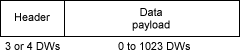
TLPs are pretty simple to interpret. Here's a general view of their structure.


The header contains 3 or 4 DWs but the most important fields are part of the first DW.


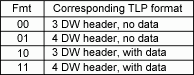
The "Fmt" field tells how long is the header, and if a data payload is present.


Then together with "Type", it describes the TLP operation. The remainder of the TLP header content depends of the TLP operation.

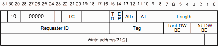
For example, here's a 32-bits memory write TLP header, where you can see that the write address is at the end of the header (and the write data is not shown as it is in the payload after the header).


The "Fmt" field is "10" which means "3 DW, with data". That makes sense, a memory write needs data to write, so upon getting the data payload after the header, we write that data to some memory (or use it somehow) and we are done with it. The Field "Length" tells how many DWs are in the payload (from 0 to 1023). Commonly, it's a single DW to write, in which case length is equal to 1 and the total TLP length is 4 DWs (3 for the header and 1 of the payload).

Now what about a memory read? Somehow we have to return data.
Completion with data

If the TLP is a memory read instead of a write, we have to execute the read and then respond. There is a special TLP for that response, it is called CplD (completion with data) and its payload contains the data that we want to return.

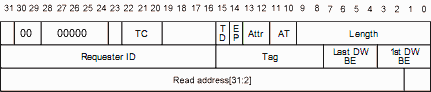
Let's take a closer look at the 32-bit memory read TLP header - it is very similar to the 32-bit memory write we had previously.


One difference is the Fmt=00, which means "no data". Makes sense, we don't need data to do a read, just an address. But we now have to respond with data. And as important, the response will need to be routed back to whoever asked for the read... Do you see the problem?

Ok, we received a read request. Did it come from the CPU? Or from the interrupt controller? Or from a graphic card? After all, many devices are capable of issuing such request. The answer is given in the "Requester ID" - it shows who requested the read. So when we create the CplD TLP, we have to recopy the "Requester ID" in it. This way, it'll be routed where it belongs by the PCI Express bridge(s). BTW, we also have to recopy the "Tag" (which is useful in case of multiple reads pending).


TLP size

A typical 32-bit address/data memory read TLP is made of 3 DWs in the header and no payload (so 96 bits total), while a similar memory write is made of 4 DWs (3 for the header and 1 for the payload). That's not very efficient in term of bandwidth because of the TLP header overhead, so it is better to use bigger TLP payloads when possible. A TLP payload can theoretically be as big as 1023 DWs, pretty handy for burst reads and writes, although PCs can limit the maximum size to a lower value (32 DWs is typical).

SiteMap